
NUS Semiconductor Club · Est. 2024

Bringing industry to learners.

Singapore builds a real share of the world's semiconductors. We're the NUS Semiconductor Club that gets you inside the cleanroom, the fab floor, the design flow, the industry

M1 · Metal 1

Companies we've worked with

  • Micron
  • Silicon Box
  • GlobalFoundries
  • SSMC
  • SSIA
  • Applied Materials
  • Marvell
  • Lam Research
  • STATS ChipPAC
  • ASM
  • ASMPT

Coming up

What's next.

  1. 2:00 pm to 4:00 pm

    Silicon Box Industry Sharing

    Sharing sessionSDE3-LT427, NUS

    Engineers and members of the HR team from Silicon Box join us to talk about what the company builds and what it looks for.

    • Silicon Box
  2. 1:00 pm to 5:30 pm

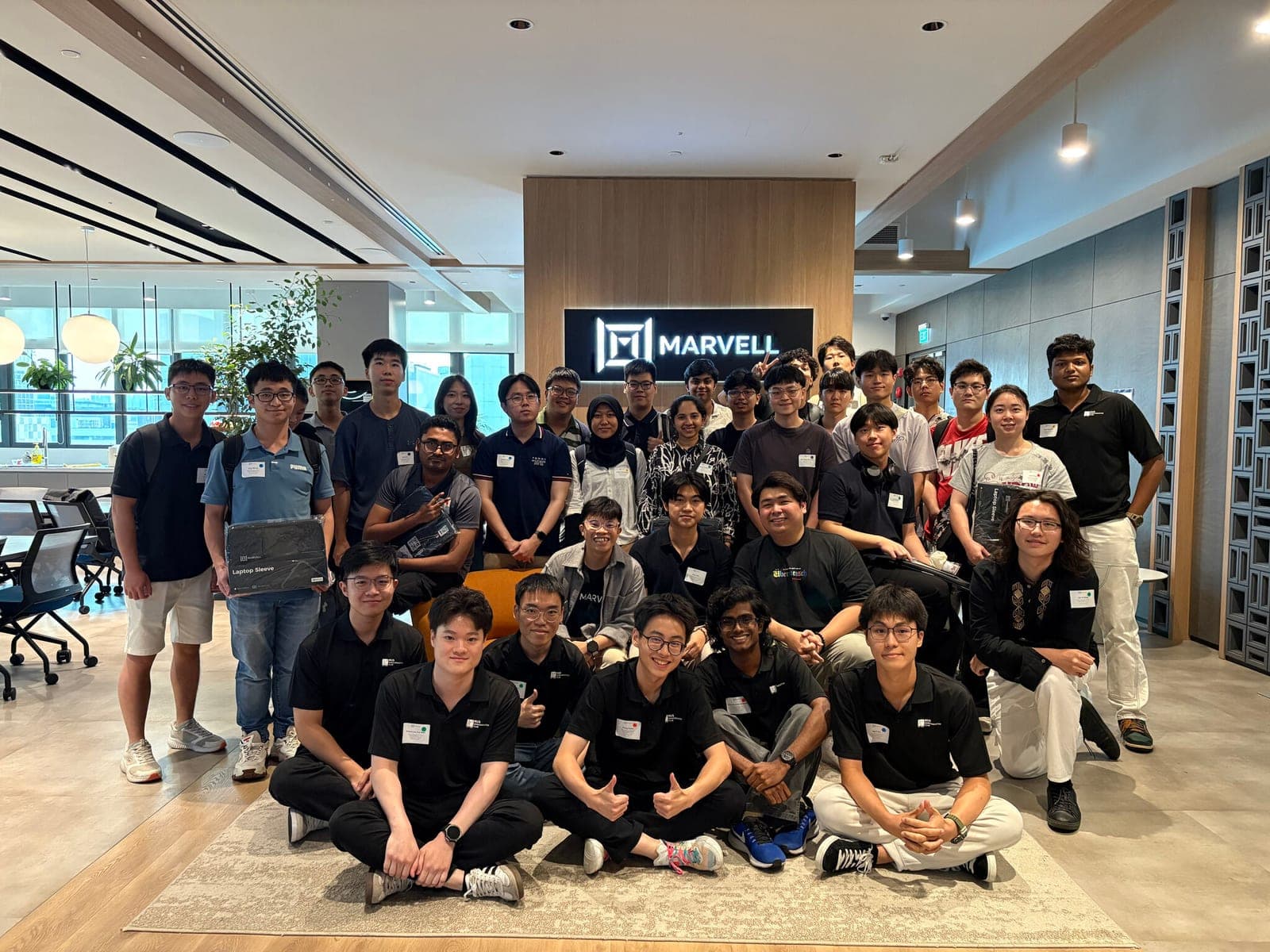
    Behind the Scenes at Marvell Technology

    Site visitMarvell Office, 3 Irving Road, Tai Seng Centre, #07-01

    An afternoon with Marvell engineers and HR, spent on the silicon behind the world's data infrastructure and on how you get into the work.

    • Marvell Technology
    • With NUS ECE Undergraduate Student Council

    Registration closed 9 Aug

Recently

Where we've been.

  1. Sharing session

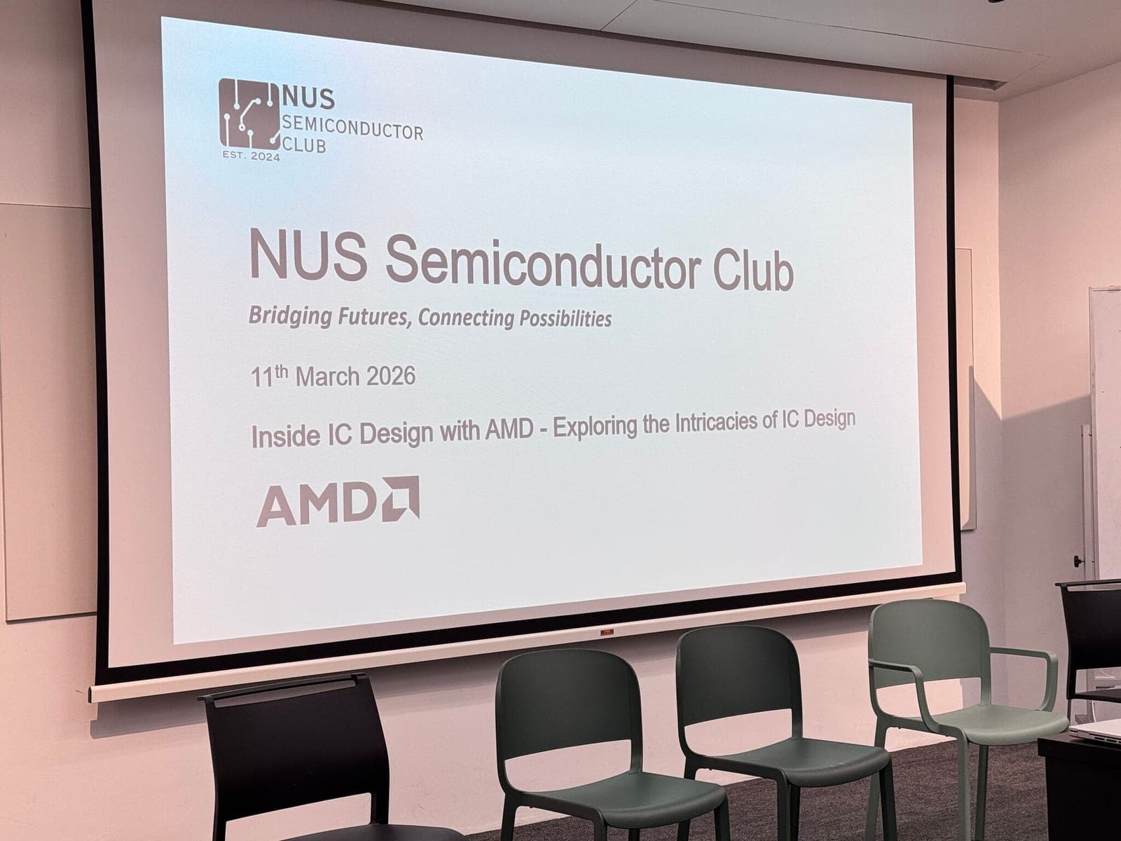
    Inside IC Design with AMD: Exploring the Intricacies of Chip Engineering

    AMD engineers walked through the full IC design flow, from architectural planning to tape-out, across digital and analog design and both front-end and back-end roles. The session went into verification complexity and the power, performance and area trade-offs engineers balance in practice, then closed with a career segment, a Q&A and networking over refreshments.

    SpeakersKwee Peng Yap, Azarudin Abdulla, Lee Wen Bin, Zi Huang Liu, Simin Xu, Catherine Ong

    • AMD
    The title slide for the AMD IC design session projected in a seminar room before the audience arrived
  2. Site visitUMC P3 Fab, Singapore

    UMC Site Visit: Manufacturing and Silicon Photonics

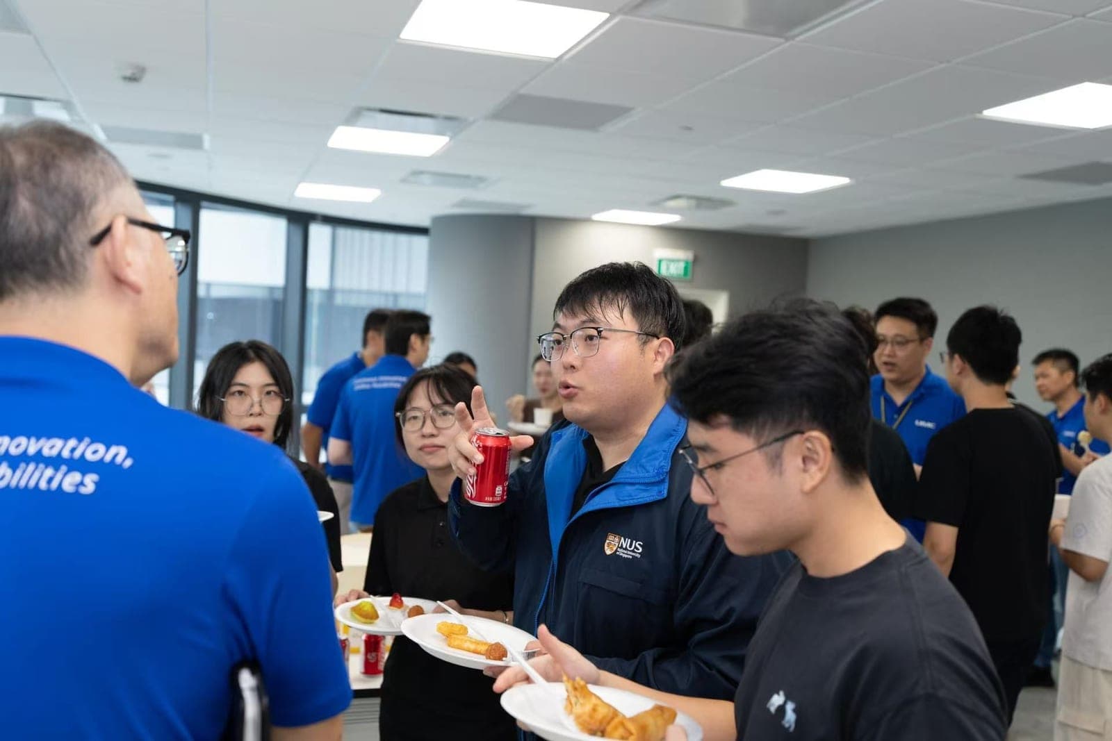
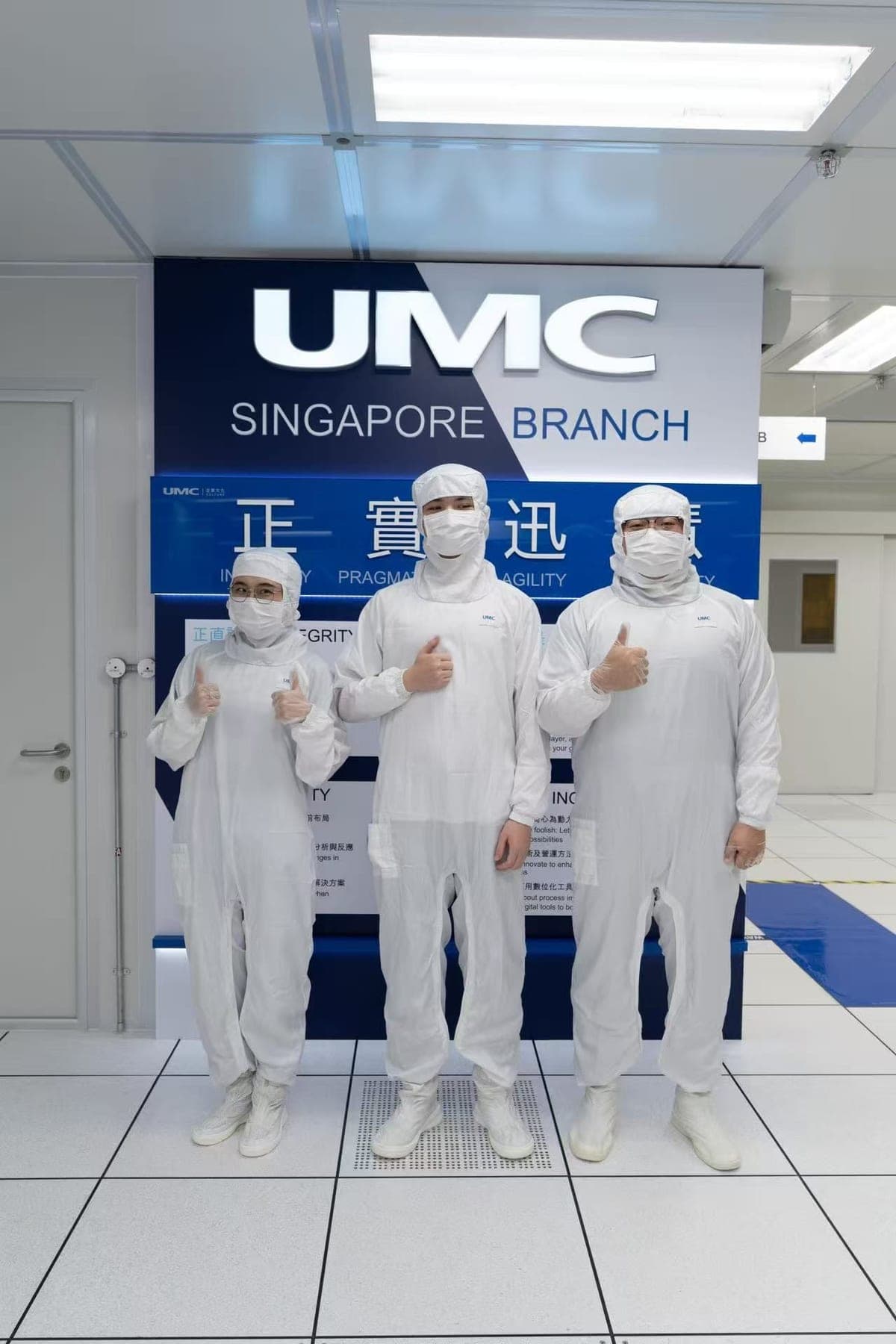
    Students toured UMC's newest P3 fab, including the cleanroom and the failure analysis labs, and saw how 22nm and 28nm production runs alongside the plant's ongoing expansion. Engineers walked through the roles behind a finished wafer, and the discussion turned to how demand for bandwidth and power efficiency is pulling silicon photonics forward. An HR sharing on career pathways and a Q&A closed the visit.

    • UMC
    Students and UMC staff talking over refreshments during the site visit
  3. Sharing session

    SemiAnalysis Sharing Session

    The SemiAnalysis team gave an overview of the global semiconductor landscape, covering advanced manufacturing, packaging and equipment, and how design and architectural choices shape AI inference performance and scalability. A segment on supply chain dynamics and cost structures connected chip design through fabrication and packaging to data centre deployment, followed by a careers section and open Q&A.

    SpeakersDaniel Nishball

    • SemiAnalysis
    Students talking beside a SemiAnalysis pull-up banner after the session
  4. Site visitAMD Chai Chee, Singapore

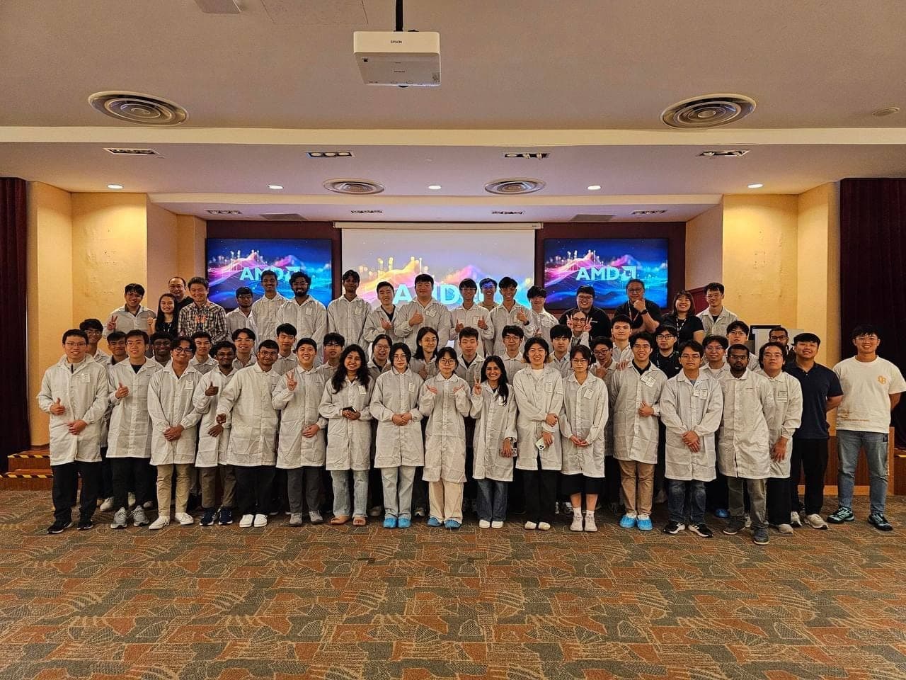
    AMD Site Visit: Behind the Scenes at AMD Singapore

    A visit spanning design, validation, testing and product support, where students saw how cross-functional teams work across the chip development lifecycle. The day covered data-driven failure analysis and the continuous test programs behind product quality, and set out where AMD Singapore sits in the company's global engineering footprint as an R&D hub. Hiring managers joined for the sharing and networking sessions.

    SpeakersCatherine Ong

    • AMD
    A large group of students in white coats posed in front of AMD screens during the site visit
  5. The archive

    Everything else we've run.

    9 events so far: fab floors and cleanrooms, the engineers who work in them, and the people who hire into the industry. Each one has a recap and photos.

    See all events

What we do

Three ways in.

The club exists to close the distance between studying semiconductors and working in them. Everything we run is one of three kinds of access.

Site visits

Get past the lobby.

We take members into the places where chips are actually made and tested. You gown up, walk the floor, and see the tools that turn a blank wafer into product. It is the fastest way to find out whether the work looks like what you imagined.

  • AMD
  • UMC Singapore cleanroom
NUS Semiconductor Club members in lab coats during a site visit to AMD

Seminars and fireside chats

Ask the people already doing the job.

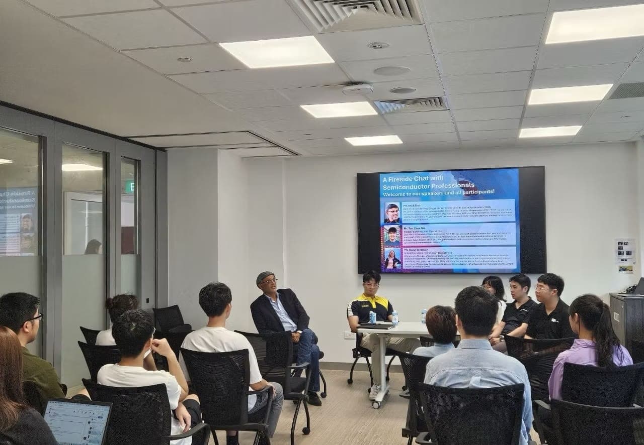
Engineers, process specialists and managers sit down with members to talk about how they got in, what the day-to-day is really like, and what they would tell a student starting now. Small rooms, real questions, no recruiting script.

  • Open to all members
  • Industry speakers
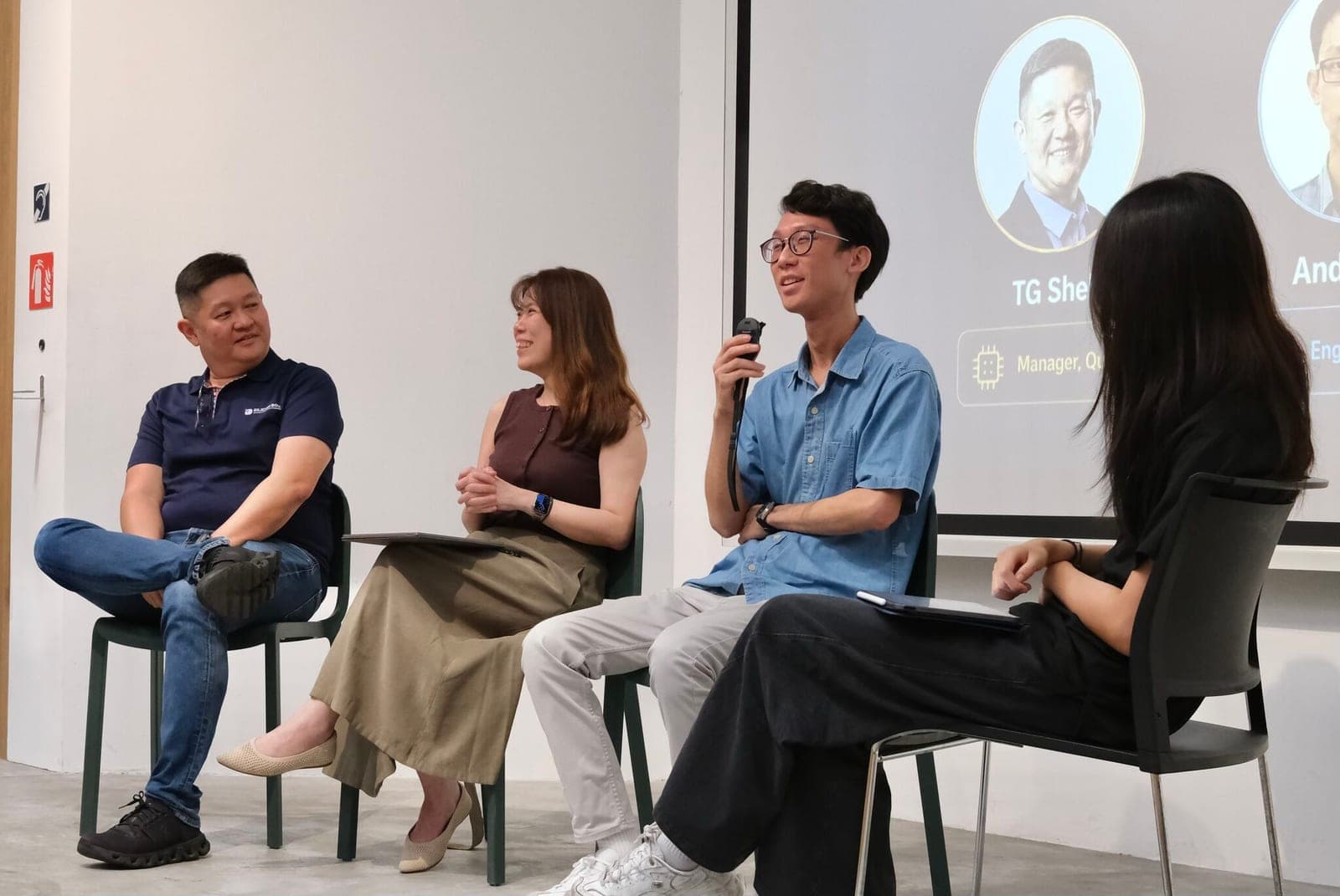
Speakers at a fireside chat with semiconductor professionals, seated in front of club members

Industry events

Be in the room.

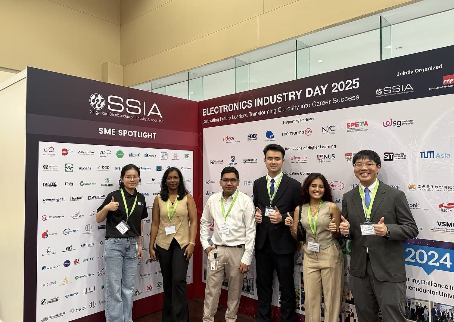
We bring members to industry days, exhibitions and networking sessions across Singapore's semiconductor scene. These are the rooms where companies, associations and the people who do the hiring actually turn up.

  • Industry days
  • Networking sessions
NUS Semiconductor Club members at a semiconductor industry day exhibition

Our community

The people behind it.

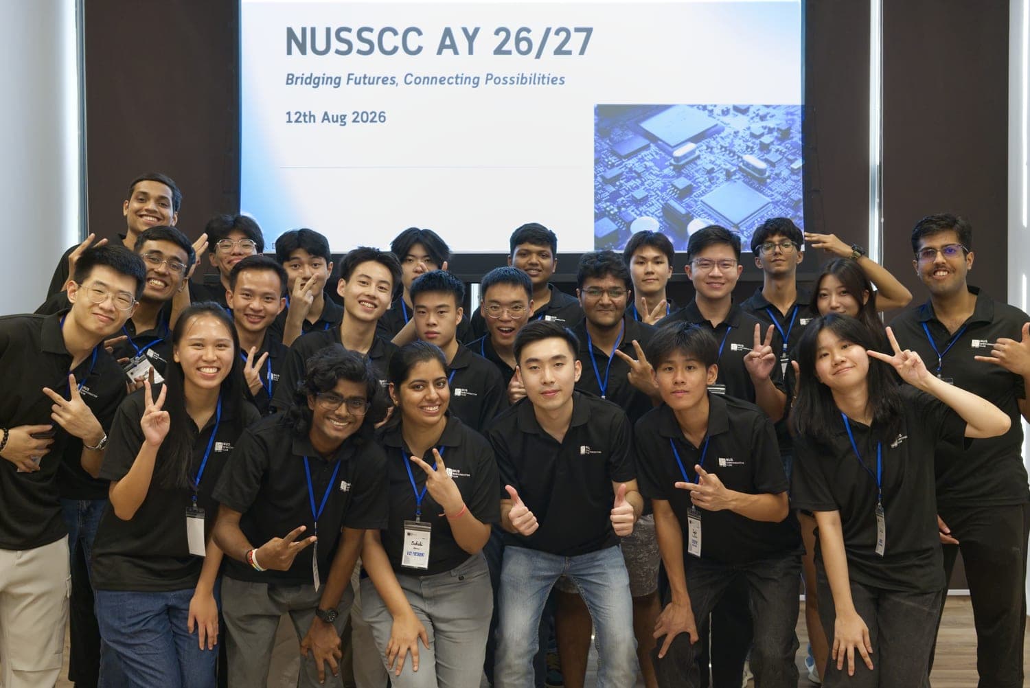
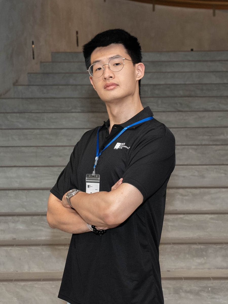
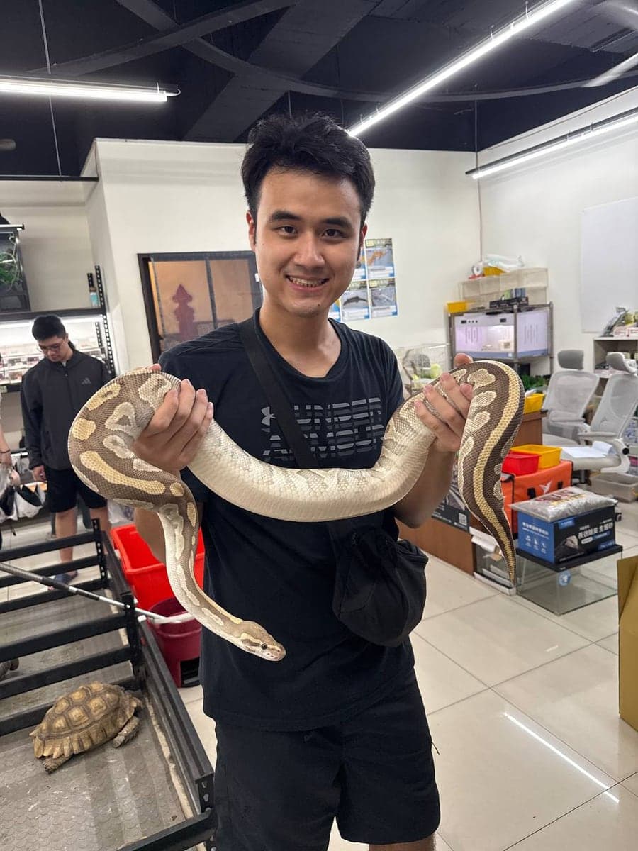
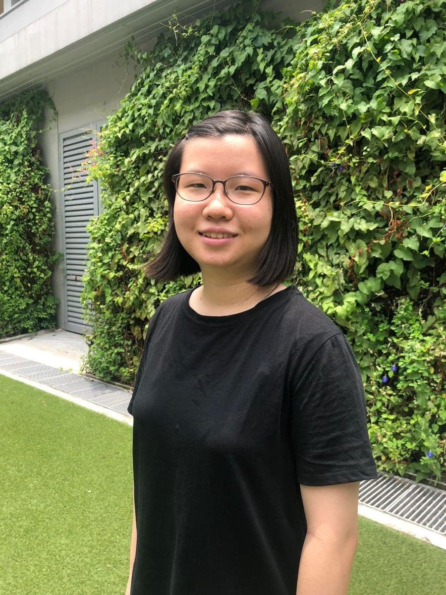
The NUS Semiconductor Club committee for AY 2026/27
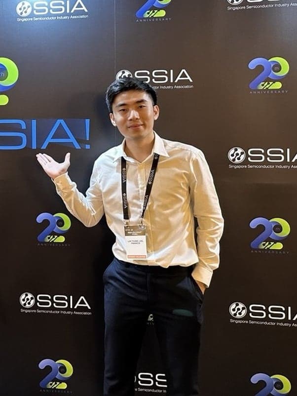
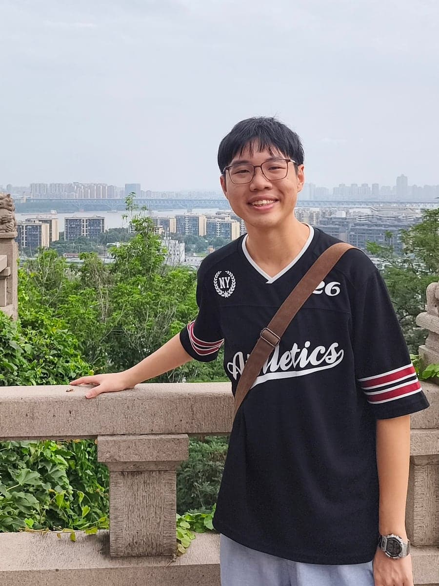
Francis Lim, president of the NUS Semiconductor Club
Most of us joined without knowing what a cleanroom looked like from the inside. What the club does is close that gap: we get you into the rooms where the work happens, and in front of the people already doing it. If you are curious about this industry, that is enough to start.
Francis LimPresident, AY 2026/27

Join us

Find out if this is your industry.

Open to any NUS student who's curious. No prior background needed. Join the Telegram and we'll tell you when the next visit or chat is happening.